 |
Home | > | Microscopy and Analysis |
|
|
|
Home | > | Microscopy and Analysis |
|
|
The Mead Testing microscopy and analysis laboratory is well equipped to assist with your failure analysis or materials characterisation needs. In addition to a suite of optical microscopes we have all the equipment required to prepare metallurgical sections and to locally remove the encapsulation from devices and integrated circuits. Optical Microscopy used in conjunction with conventional metallurgical sectioning can often solve material or component problems quickly, efficiently and at a low cost. This technique permits measurement of plating thickness, solder and material grain structures and the distribution of intermetallic layers all of which are crucial to solder joint reliability. Our microscopes incorporate digital image capture allowing us to quickly report results.
|
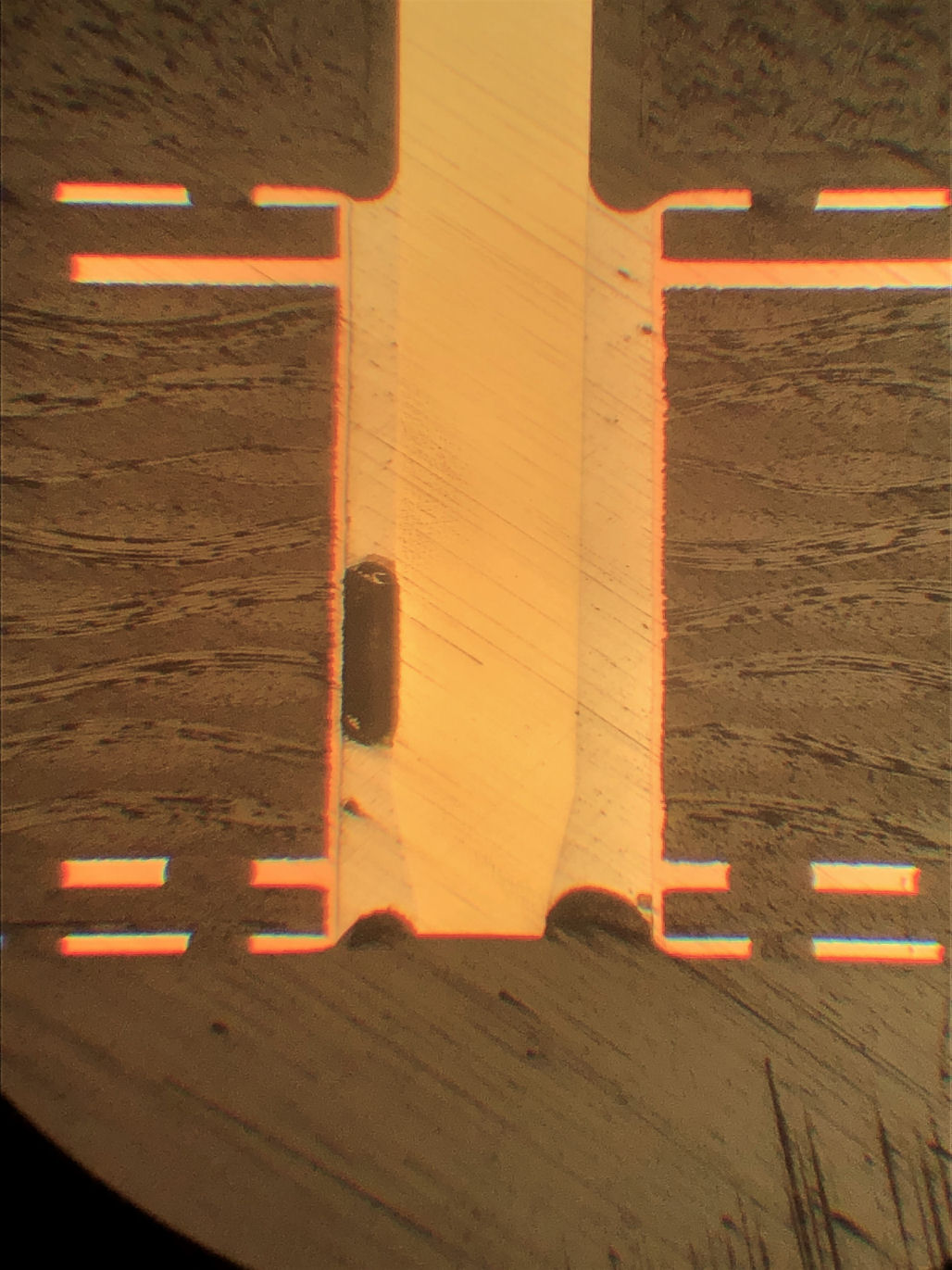
Optical micrograph of a sectioned solder joint showing voiding in the solder fillet |
|
|
|